NVLink, NVSwitch
When distributing LLM training across 8 GPUs within a single server, each GPU must perform an All-Reduce operation in every step, exchanging the gradient data it calculated with all 7 other GPUs.
What kind of physical breakdown occurs if this massive communication traffic is routed through the existing motherboard's PCIe bus, and how is a dedicated network designed to bypass this?
In a multi-GPU environment, the core of performance lies not in the computational power of a single GPU, but in the Interconnect architecture that determines how quickly and losslessly data can be transferred between GPUs.
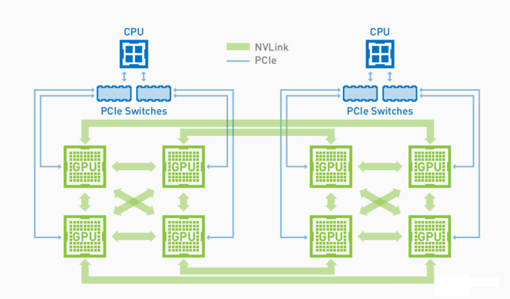
NVLink #
To bypass the physical limitations of the existing PCIe bus, NVLink is a high-speed P2P hardware interconnect technology that directly connects GPUs without going through the motherboard's underside, either via the top or a dedicated baseboard (SXM).
NVSwitch #
As the number of GPUs within a single server increases to 4 or 8, it becomes impossible to connect all GPUs 1:1 in a full mesh due to physical pin count limitations.
To solve this, NVSwitch is a dedicated routing ASIC chip installed inside the server, providing a fully non-blocking crossbar architecture that guarantees maximum bandwidth without bottlenecks for communication between any GPUs.
SXM (Server PCI Express Module) Form Factor #
Unlike typical graphics cards that plug vertically into motherboard PCIe slots, this is an enterprise-exclusive form factor where GPUs are mounted horizontally and closely on a dedicated motherboard with an integrated NVSwitch. The physical NVLink pins are wired through this board.
Problem Definition #
When performing multi-GPU distributed training relying on PCIe topology, critical bottlenecks occur at the data link layer.
- Bandwidth Mismatch: The HBM bandwidth inside a GPU reaches 1.5~3TB/s, but the maximum bidirectional bandwidth of a PCIe Gen4x16 lane for external transfer is only 64GB/s. This creates an extreme I/O bottleneck where computation finishes in 1 second, but data exchange takes 30 seconds.
- PCIe Switch Root Complex Congestion: If 8 GPUs broadcast data simultaneously, all traffic converges on the motherboard's PCIe switch. Bus contention leads to packet collisions and queue saturation, causing latency to increase exponentially.
Solution #
NVIDIA did not completely abandon the PCIe bus but built its own dedicated hardware communication network within the server to expand communication bandwidth.
- Maximizing Bandwidth through Multi-Lane Bonding: NVLink is not a single physical wire but consists of multiple high-speed serial links. An A100 Tensor Core GPU has 12 NVLinks, which combined provide a physical bandwidth of 600GB/s bidirectional, approximately 10 times wider than PCIe.
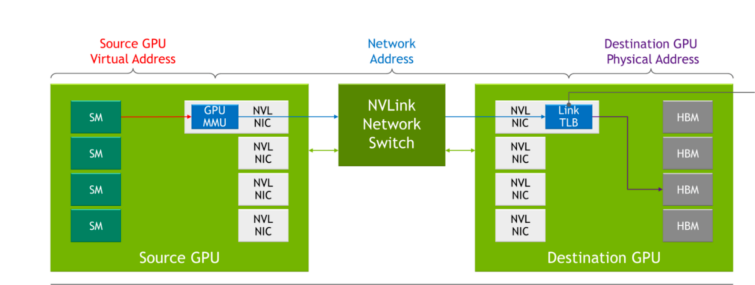
- Unified Memory Architecture: NVLink is not merely a network cable that copies and transfers data. It is interconnected at the physical memory controller level, allowing a thread on GPU0 to issue direct load/store commands to the HBM memory address (Remote Memory) of GPU1, as if it were its own local memory.
How it Works #
Let's trace the hardware data path when tensor data calculated on GPU0 is transferred to GPU7.
(Based on SXM and NVSwitch environment)
- From Shared Memory to NVLink Controller: The final gradient data generated by the SM (Streaming Multiprocessor) compute cores of GPU0 is flushed to the L2 cache. The data is then transferred to the dedicated NVLink MAC/PHY block located on the periphery of the GPU chip, not the PCIe PHY (physical layer).
- Output from GPU Chip (Entry into SXM Baseboard): Data packets are converted into electrical signals and pour into the copper wiring inside the motherboard (SXM baseboard) through ultra-high-density pins at the bottom of the GPU chipset.
- NVSwitch Routing (Crossbar Traversal): The electrical signals enter the NVSwitch ASIC chip soldered onto the baseboard. The NVSwitch physically performs Circuit Switching between the input port GPU0 and the destination port GPU7 via its internal logical crossbar circuit. During this process, there is no interference with communication between other GPUs, such as GPU1 -> GPU2.
- Arrival at Destination GPU HBM: The routed signals travel back through the baseboard's wiring to GPU7's NVLink PHY, pass through the memory controller, and are directly written to GPU7's HBM memory. All of this occurs with zero host CPU intervention.
System Low-Level Metrics and Profiling Log Analysis #
These are terminal commands and output logs that an engineer can use to check the physical connection status and bandwidth status of NVLink by accessing the server.
root@ai-server:~# nvidia-smi nvlink -s

GPU 0: NVIDIA A100-SXM4-40GB
         Link 0: Data Rx: 23154 MB, Data Tx: 23154 MB
         Link 1: Data Rx: 23153 MB, Data Tx: 23153 MB
         ...
         Link 11: Data Rx: 23154 MB, Data Tx: 23154 MB
GPU 1: NVIDIA A100-SXM4-40GB
         Link 0: Data Rx: 23154 MB, Data Tx: 23154 MB
...
- This indicates that all 12 physical NVLinks (Link 0 ~ 11) on a single GPU are active and operational.
- If the
Data Rx(receive) andData Tx(transmit) values are uniformly increasing for each link, it proves that the hardware topology is perfectly balanced via NVSwitch and that distributed training communication traffic is flowing normally through NVLink. If the value is 0 or missing for a specific link, a hardware defect (cable disconnection or pin failure) should be suspected.
Profiling/Configuration #
This describes environment variable tuning techniques to check if the distributed training library NCCL (NVIDIA Collective Communications Library) has selected NVLink as the hardware network in an AI infrastructure environment, and to enforce it.
Activating NCCL Debug Logs and Diagnosing the Network: When running a PyTorch DistributedDataParallel (DDP) training script, increase the debug level to analyze the hardware routing tree at the software layer.
# NCCL 내부의 채널 생성 및 프로토콜 선택 로그 출력
NCCL_DEBUG=INFO python distributed_train.py
Key log lines to check in the terminal are:
ai-server:1234:1234 [0] NCCL INFO Channel 00/12 : 0 1 2 3 4 5 6 7
ai-server:1234:1234 [0] NCCL INFO Using internal Network NVLink
If this log outputs Using internal Network PCIe or SHM(Shared Memory), it indicates a critical state where the NVSwitch configuration is broken, or the NVLink driver is not recognized due to insufficient host IPC (Inter-Process Communication) and hardware volume mount permissions when running the Docker container.
Forcing PCIe Communication Blockage can also be done.
If NVLink exists in the system but you want to completely prevent the mixed use of PCIe due to software bugs or configuration issues, you can do the following:
# 피어투피어 통신 시 PCIe(P2P) 경로 사용을 명시적으로 비활성화하고 NVLink만 사용하도록 강제
export NCCL_P2P_DISABLE=0
export NCCL_P2P_LEVEL=NVL